
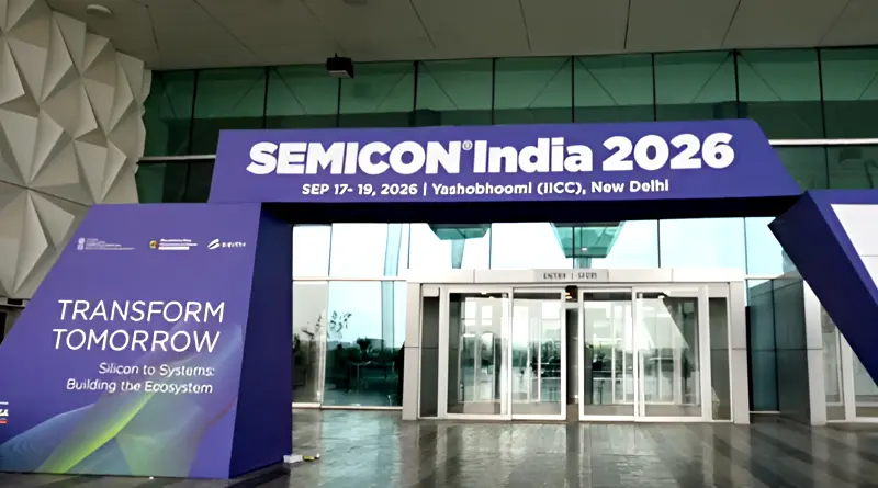
Semicon India 2026: India’s Growing Semiconductor Value Chain

Semicon India 2026, organized by India Semiconductor Mission and SEMI at Yashobhoomi, New Delhi, featured over 500 companies and attracted a footfall of around 40,000 industry professionals. The three-day event was held from 17th to 19th September.
Companies at the event showcased capabilities ranging from chip design, compound wafer fabrication, machinery for semiconductor production, specialty chemicals, and gases for cleanroom processes.
L&T Semiconductor: Designing Indigenous Chips
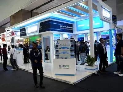
A major highlight of the exhibition was L&T Semiconductor Technologies Limited (LTSCT), a wholly owned subsidiary of Larsen & Toubro Ltd. (L&T), demonstrating India’s growing indigenous chip designing capabilities.
At its booth, LTSCT showcased its designs of compound semiconductors, presenting processed Silicon Carbide (SiC) wafers and chips fabricated from it for various applications. The chips included 1,200V SiC MOSFETs and 6-in-1 SiC Intelligent Power Modules (IPMs). These SiC chips are designed to perform at high voltage and temperatures, with minimal power loss. These components have applications in electric vehicle (EV) traction inverters, DC fast chargers, solar inverters, and power grids.
The company displayed processed wafers of an indigenously designed BLDC motor controller with tape-on-ring. This controller chip has a flexible architecture that allows it to be used across multiple BLDC fan products.
LTSCT also displayed AI-enabled Smart Vision System-on-Chip (SoC) and Secured Identity Chip. Smart Vision SoC is used for intelligent surveillance cameras and automated industrial optical inspection systems. Further, the Security Identity Chip has cryptographic acceleration and hardware-rooted security, and is initially designed for e-Passports, payment cards, and national ID systems.
LTSCT’s representative in talks with CableCommunity said that as these products’ designs and Intellectual property reside locally, it helps curb dependence on imports. He also mentioned that the company will serve both domestic and global customer markets.
Tata Electronics Signs Multiple MoUs at Semicon India 2026

Tata Electronics, at Semicon India 2026, signed a total of 16 Memoranda of Understanding (MoUs), building a supply chain for its upcoming fabrication facility in Dholera, Gujarat. This facility will manufacture 300mm chips with process nodes ranging from 28nm to 110nm, with applications across automotive power management ICs (PMICs), display drivers, mobile devices, and AI hardware.
Tata signed an MoU with LTSCT; under this collaboration, LTSCT’s indigenously developed semiconductor designs will be fabricated at Tata Electronics’ Dholera Fab Facility. “Our partnership… will accelerate India’s vision of becoming a full-stack semiconductor nation by combining L&T Semiconductor’s deep fabless design and engineering expertise with our capabilities across semiconductor manufacturing, packaging and testing”, said Dr. Randhir Thakur, CEO & MD, Tata Electronics.
Other major MoUs include partnerships with Japan’s Sumitomo Chemical and Fujifilm. With Sumitomo, Tata secures supply of essential materials, including advanced photoresists, functional process chemicals, and ultra-high-purity (UHP) chemical agents critical for photolithography and wafer cleaning. The agreement with Fujifilm focused on the development and supply of advanced semiconductor materials tailored to the requirements of Tata Electronics’ upcoming semiconductor Fab in Dholera, Gujarat. Fujifilm’s upcoming facility for manufacturing semiconductor materials will be developed in Dholera, making this close proximity beneficial for both companies.
Global Semiconductor Equipment Suppliers Backing India’s Fabs
Semiconductor Manufacturing machinery suppliers were another major highlight of the exhibition. Companies, including ASML Holding N.V., Applied Materials, Inc., and Tokyo Electron Ltd. (TEL), were at the event and said that they will supply production machinery to Fabrication facilities in India. The companies, in conversation with CableCommunity, said that their current Indian partner is Tata Electronics, where this customer base may expand considering India’s growing semiconductor segment.
ASML To Supply its Holistic Lithography Tools
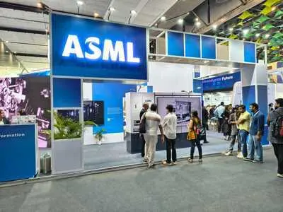
ASML, a Dutch supplier of photolithography systems to the semiconductor industry, was present at the exhibition. The company showcased its Lithography tool, TWINSCAN NXT:1980Di, i.e. ArF (Argon Fluoride) Deep Ultraviolet (DUV) immersion lithography system used for high-volume manufacturing of logic and memory chips, and novel chip innovation.
Company’s other machinery products from its holistic lithography portfolio include EUV lithography systems that enable chipmakers to print more transistors onto a single chip.
Applied Materials Announces USD 5 Bn Investment
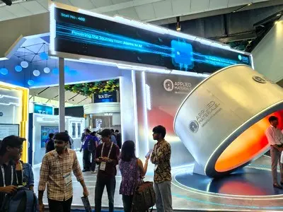
US-based Applied Materials’ executive said to CableCommunity that they have a range of machinery to produce any sort of semiconductor chip and will supply as per requirement. The company’s product portfolio includes atomic layer deposition (ALD), physical vapor deposition (PVD), and chemical vapor deposition (CVD), alongside advanced CMP planarization systems. These machines are designed to deposit atomic-scale dielectric and metallic films onto wafers and mechanically polish them between process layers.
Further, the company has products for Ion implantation and etch systems that are precision tools to remove unwanted materials from silicon wafers at atomic level.
At Semicon India 2026 conference, Mr. Prabhu Raja, President, Semiconductor Products Group at Applied Materials, announced a USD 5 billion investment over the next decade, including a 140-acre advanced semiconductor research park. This plan also includes expansion of India-based supply chain capacity.
Tokyo Electron to Supply Etching and Wafer Fab Machinery
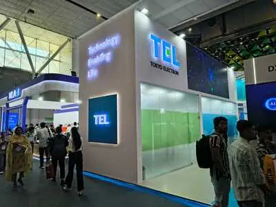
Tokyo Electron (TEL) at the event displayed machinery including coater/developer track systems, CLEAN TRACK™ LITHIUS Pro™ Z, which coats silicon wafers with photosensitive chemicals prior to lithography exposure and washes away the exposed areas afterward to finalize circuit pattern.
The company’s portfolio also includes plasma etch and thermal processing systems. These systems selectively etch any unwanted materials, which helps define microscopic circuit features and anneal processed wafers, enabling activation of electrical properties. The company will supply these tools to Tata Electronics.
SiCSem’s Upcoming Compound Fab & ATMP Facility in Odisha
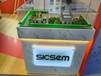
SiCSem Private Limited at the exhibition showcased a model for its upcoming Compound Fab & ATMP Facility in Odisha. In a talk with CableCommunity, the company executive said that this facility will manufacture compound semiconductors, such as Silicon Carbide and Gallium Nitride wafers, to fabricate microchips, Diodes, and SiC MOSFETs.
These products are designed for high-power applications in Electric vehicles (EVs), super-fast DC chargers, Renewable energy systems and solar power inverters, Defence equipment, aerospace, and missiles, Data center racks, high-speed rail, and industrial power supplies.
The facility, being built on 22 acres of land, will have an annual capacity of 60,000 wafers and a packaging capacity of 96 million units per year.
FujiFilm’s Rs. 800 Cr facility in Dholera, Gujarat
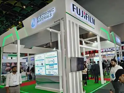
Fujifilm Corporation, a Tokyo-based semiconductor material supplier, will set up a manufacturing facility in India. The company’s executive, in talks with CableCommunity, said the Rs. 800 crore investment will be in two phases. In Phase 1 the company will focus on semiconductor process chemicals, and in Phase 2 it will expand into surface conditioning materials and high-purity chemicals.
The company currently supplies semiconductor materials from its overseas facilities and, seeing India’s growing semiconductor facility have decided to set up a local semiconductor material manufacturing system.
INOXGFL Showcases Range of Fluoropolymers, Specialty Chemicals and Gases
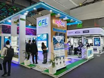
INOXGFL, an Indian manufacturer and supplier of chemicals and polymers, presented its range of fluoropolymers, specialty chemicals, and cleanroom process gases for the semiconductor supply chain.
Some of the Fluoropolymers the company showcased included INOFLON PFA (Perfluoroalkoxy alkane) polymers, INOFLON PTFE (Polyfluorotetraethylene) polymers, and INOFLAR PVDF (polyvinylidene fluoride) polymers. These polymers offer high chemical resistance and are used to manufacture fluid-handling components such as tubes, pumps, valves, and fittings in semiconductor manufacturing processes.
INOXGFL Specialty Chemicals and Gases
Further, the company displayed specialty chemicals, such as Anhydrous Hydrogen Fluoride (AHF), for Native oxide removal, wafer surface preparation, and selective cleaning of silicon-based materials. Perfluoropolyether (PFPE) is a specialty fluid for high-vacuum lubrication of wafer-handling robots, bearings, and semiconductor process equipment.
INOXGFL presented Nitrogen Trifluoride (NF3) Flourine/Nitrogen Mix (F2/N2), which are chamber cleaning gases. Where, NF3 is used for cleaning Chemical Vapor Deposition (CVD) reactors in semiconductor fabs without damaging the hardware. F2/N2 is used for chamber cleaning and surface modification, while also reducing the Global Warming Potential (GWP) footprint.
Semiconductor Ecosystem Growing Beyond Fabrication & Packaging
India’s semiconductor sector is growing rapidly; this was hinted at by the increase in exhibitors at the event compared to the previous edition. The event highlighted a diverse and evolving semiconductor value chain, from indigenous front-end chip design and IP to fabrication and back-end packaging, testing, and also critical supply chains including specialty chemicals and gases for cleanrooms.
Moreover, Global companies belonging to different parts of the value chain showed interest in actively participating in India’s emerging semiconductor market.
